Past Events
Industrial Applications of Ultrafast Lasers II: Illustrative Examples
As a follow-up to Seminar I, I will discuss specific examples of fs UPS and photovoltage experiments on industrially relevant materials and stacks. Aside from single crystal Si wafers, virtually all materials found in MOS devices, photovoltaics, oxides, organic films (OLEDs, resists) and phase change materials, are polycrystalline or amorphous. Angle integrated UPS provides high count rates that increase sensitivity useful for identifying defect state densities in materials.
A Matter of Mystery
Abstract: Neutrinos are enigmatic particles. Their properties are rather basic and yet so bizarre and surprising that at times we hardly believe them. We barely notice their presence, and yet they are everywhere and are essential to things as glaring as the sun’s energy production. The minuscule but non-zero mass of a neutrino, nearly a million times smaller than the electron (the next lightest particle), has enormous consequences for our understanding of these particles and their role in shaping the universe.
Search for New Physics with Electron Dipole Moments
A major goal of modern particle physics is to search for phenomena that are in conflict with our best theoretical understanding of nature, the Standard Model (SM). One approach in the search occurs at the laboratory scale where the SM’s most precise predictions are tested by the most precise measurements of fundamental particles. Deviations at this high-precision frontier would inform the search for Beyond the SM (BSM) physics.
TBA
Industrial Applications of Ultrafast Lasers I: Basic Physics and Examples
CU Boulder · JILA X317 | UC Berkeley · Birge 468 Critical to the design and development of present and future semiconductor and quantum devices is the full understanding of the electronic structure of the materials that comprise the complex functional stacks in a non-destructive way. In Seminars I and II, I will describe the application of femtosecond ultraviolet photoelectron and photovoltage spectroscopy (fs UPPS) to fully characterize the electronic structure of industrially important materials and devices.
TBA
Molecular Quantum Information Science with Electron Spins
Abstract: Quantum technologies based on molecules afford unique potential in miniaturization, spatial localization, and tunability through synthetic chemistry. Paramagnetic molecules constitute a platform for implementing quantum bits (qubits) and quantum sensors (qusors). While electron spin decoherence can potentially be leveraged in quantum sensing applications, its use is ultimately limited by spin relaxation, which effectively leaks quantum information into the environment.
Galaxies in extreme environments
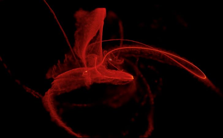
Abstract: Galaxies are a lot like people. If you pay attention to someone’s accent, mannerism, music taste, and cuisine preference — you can infer something about their culture, their heritage, their ancestry. On the same vein, by inspecting a galaxy’s morphology, kinematics and chemical composition — one can infer information about its assembly history, its interaction history. The first part of this talk will focus on extreme galactic collisions, where a small satellite crashes onto the baryonic body of a massive neighbor and survives.
Two tales about time in living (and not-so-living) transport networks
Abstract: We utilize transport systems daily to commute, e.g. via road networks, or bring energy to our houses through the power grid. Our body needs transport networks, such as the lymphatic, arterial or venous system, to distribute nutrients and remove waste. If the transported quantity is information, for example carried by an electrical signal, then even the internet and the brain can be thought of as members of this broad class of webs.
Generating quantum correlations between light and microwaves with a chip-scale device
TBA
New opportunities in metrology and quantum science with multi-electron atoms: superradiant lasers, 2D dipolar supersolids, and optical tweezer arrays.
Abstract: Cold atoms provide an ideal platform for many aspects of quantum science, from metrology to simulation to quantum computing and networking. These applications stem from their status as simple quantum objects, whose degrees of freedom can be controlled and entangled, and whose properties are identical and constant.
Nanoscale X-ray Imaging Capabilities at NSLS-II and Their Application to Microelectronics Research
National Synchrotron Light Source II (NSLS-II) has world-leading nanoscale X-ray imaging capabilities. The Full-field X-ray Imaging (FXI) beamline offers nanoscale tomography at ~30 nm resolution with an unprecedented imaging throughput down to ~10 seconds. The Hard X-ray Nanoprobe (HXN) beamline delivers multimodal X-ray imaging based on scanning X-ray microscopy with the smallest beam size of ~10 nm. In addition, additional imaging beamlines are either under construction or being designed to further strengthen the imaging portfolio at NSLS-II.


