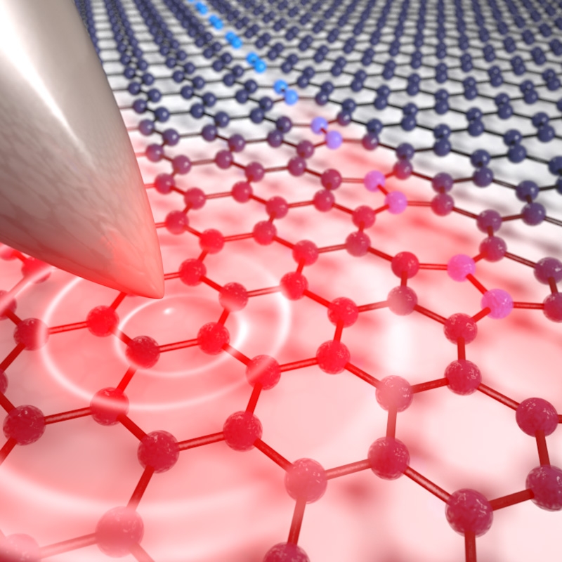
The Raschke group recently came up with a clever way to detect folds and grain boundaries in graphene. a sheet made of a single layer of carbon atoms.Such defects stop the flow of electrons in graphene and are a big headache for engineers working on touch screens and other electronic devices made of this material.
The group has invented a nano sonar-like system that uses infrared (IR) light waves (instead of water waves) to find flaws in graphene. An innovative setup creates a “virtual” optical cavity between an atomic force microscope (AFM) tip and a defect boundary. When the AFM tip emits infrared (IR) light waves across the surface of graphene, the defect boundary reflects them back across the surface to the tip, creating a standing wave. The scattering of the standing wave by the AFM tip is then captured and imaged with an IR nano microscope, showing the defect boundary. The process generates snapshots of the fatal flaws that impede the transport of electrons and light in graphene.
The group recently conducted a detailed analysis of both the amplitude and phase of the IR surface waves in its new detection system. The analysis allowed the researchers to locate flaws in the material that would affect device performance. At the same time, they were able to come up with a simple, straightforward theory to describe the surface waves they measured.
In a test of graphene of the type under development for touch-screen sensors, the group found an unexpectedly large number of boundary defects. This result was a surprise because the sample was supposed to be of high quality, and previous tests had failed to detect similar defects. Nevertheless, it was “back to the drawing boards” for industry engineers—except that now, thanks to the Raschke group, they can use the group’s relatively simple method to test for boundary defects.
The researchers responsible for this new method include CU undergraduate Justin Gerber (who dreamed up the virtual optical cavity), research associate Sam Berweger, Brian T. O’Callahan, and Fellow Adjunct Markus Raschke.
This work is important because of the high hopes for graphene-based electronics. This ultrathin material is surprisingly strong and flexible. And, it appears to have just the right electronic properties for use in flexible displays, touch sensors, photosensors, and other devices. Researchers are even investigating ways to use graphene to make basic circuit elements such as transistors. However, a serious stumbling block to realizing the potential of graphene is the ability to produce sheets of high enough quality for graphene to live up to its reputation.
The new technique developed by the Raschke group is an important step in this direction because it can detect folds and grain boundaries both before and after graphene is made into a device. Plus, the surface waves used in the technique may also lead to applications for future high-speed electronics! – Julie Phillips