
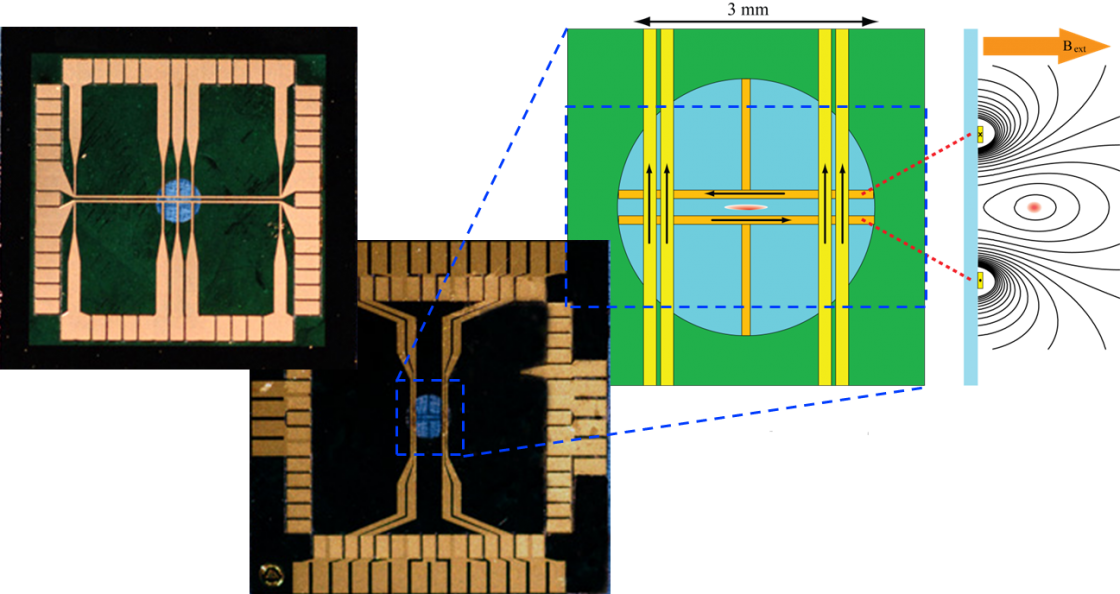
At the heart of the atomtronics experiment is our window atom chip technology (shown below). By patterning wires directly over the chip window it becomes possible to produce samples of ultracold atoms extremely close to a surface with high numerical aperture optical access. Below is an example of one of our “split-wire” atom chips, which enables trapping of atoms in an H-trap such that the atoms sit in a cigar-shaped trap arbitrarily close to the window.
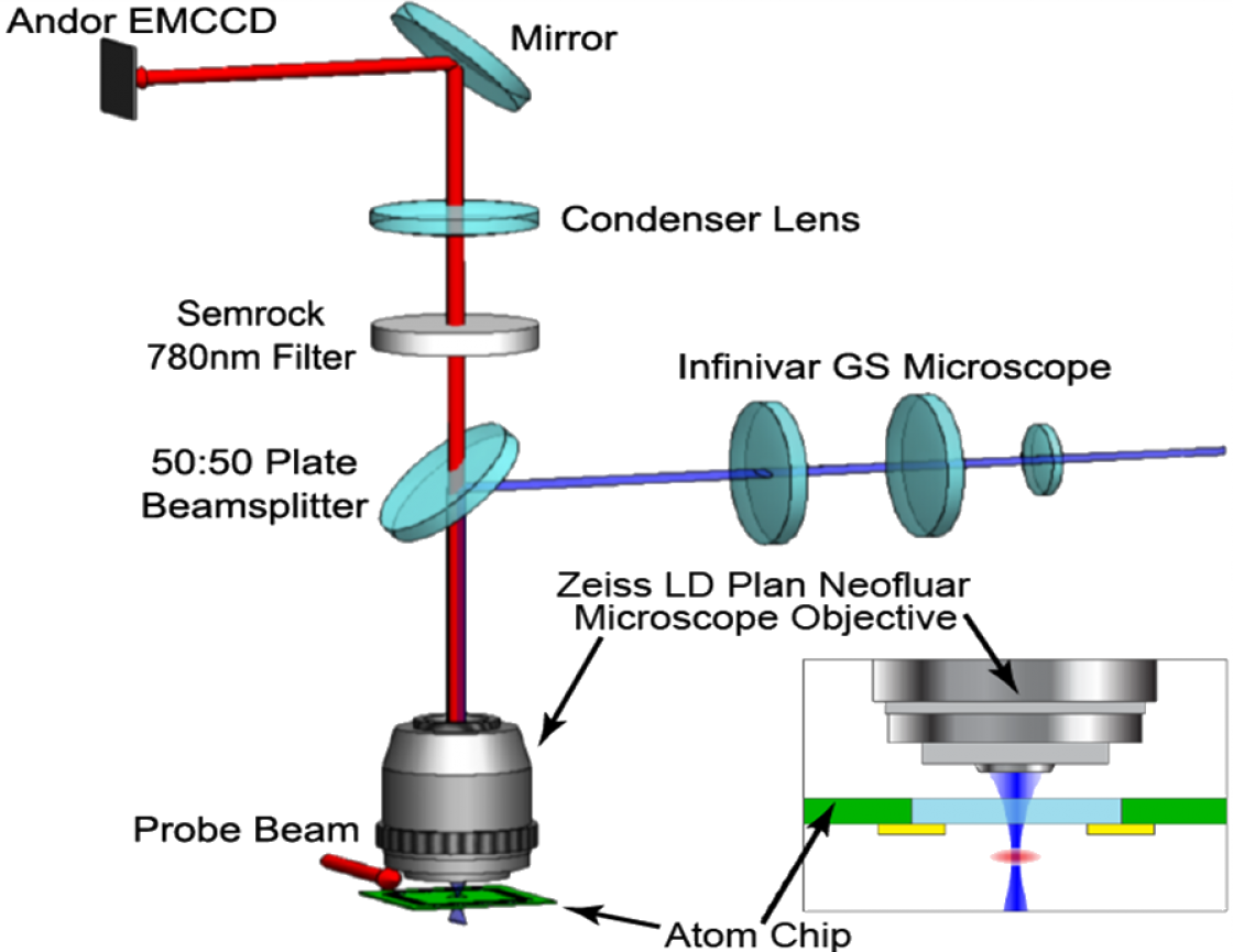
The optical window affords us significant versatility in regards to imaging and optical manipulation of magnetically trapped ultracold atoms. To this end we have developed a high numerical aperture microscope system from commercially available components for simultaneous optical projection and imaging. With our current atom chip design we can, in principle, work at numerical apertures of up to 0.9 enabling both high resolution imaging as well as the projection of high spatial bandwidth optical landscapes. Shown below is a schematic representation of this microscope system. Note that all of the optics necessary for high numerical aperture optical access are placed outside of the vacuum chamber eliminating the need for custom in-vacuo optical systems.
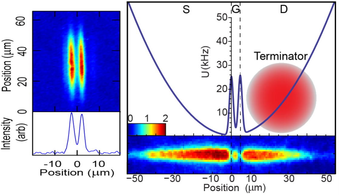
Using this setup we have recently demonstrated the function of a matterwave transistor oscillator, which is a fundamental component in atomtronics technology. To do this we superimpose two blue detuned light sheets onto the atom chip magnetic waveguide potential to form a triple-well geometry. Shown below and left is the profile of these barriers imaged using our microscope assembly. Shown below and right is the overall potential along with an in-trap absorption image of an ultracold atom cloud occupying all three potential wells. Borrowing from field-effect transistor nomenclature, we describe the potential wells as “source,” “gate” and “drain” labeled along the top by S, G and D, respectively. Additionally, an optical pumping beam, deemed a “terminator” beam, is positioned overlapping the drain well in order to couple tunneled atoms to the vacuum field. The purpose of the terminator beam is to eliminate any feedback effects resulting from the build-up of chemical potential in the drain well by pumping the tunneled atoms into a magnetically untrapped state.
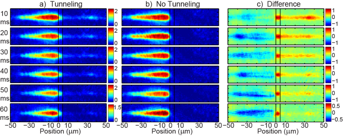
The figure below shows averages of 10 in-trap absorption images detected by our high resolution imaging system. Similar to the figure above, the source well is on the left, the gate well is in the middle, and the drain well is on the right. The vertical black lines represent the centers of the two optical barriers. Initially, all atoms are confined in the source well. Shown in (a) is a series of images that capture the emitted matterwave over a period of 60 ms. Note that the terminator beam is removed prior to imaging for a time equal to about twice the magnetic trap oscillation period to allow the matterwave to be captured in the drain well. Thus, the drain well acts as a sort of spectrum analyzer since a peak in optical density is recorded at a position corresponding to the energy of the matterwave. Given the curvature of our magnetic potential we find that the matterwave has an energy of approximately 22 kHz. As time evolves the driving potential becomes depleted and the output of the oscillator decreases. The series in (b) is a control case where the optical barriers are either high enough or the gate region is narrow enough to inhibit tunneling. Finally, in (c) the subtraction of series (b) from (a) better illustrates the matterwave output along with the location from which atoms tunnel out of the source well.
It is interesting to see how the process of tunneling affects the atoms in the source well. As the transistor oscillates the difference in chemical potential between the source and gate, μsg, and therefore the junction resistance, R, are negative. The observed result is additional cooling of the atom cloud as seen in the figure below where the data points are determined from time of flight absorption imaging. Given the fact that the power dissipated is given by Pd = I2R, a negative resistance corresponds to negative power dissipation, or ohmic cooling. In our case this leads to an increased rate of condensation of the source atoms. The blue trace refers to the case where tunneling is allowed and the red trace represents the control case where tunneling is inhibited.