Two-dimensional materials, like graphene and 2D semiconductors, are an area of physics that has been growing tremendously in the last decade. According to JILA graduate student Ben Whetten, “That’s because they exhibit new spin and electronic physical phenomena and have much promise to build new miniaturized photonic or semiconductor nanoscale devices.” Researchers like Whetten, and his advisor, JILA Fellow, and University of Colorado Boulder professor Markus Raschke, develop methods to image these materials, giving a better understanding of their inner workings. In a new paper in NanoLetters, Raschke, and his team extended their ultrafast microscope to see nanometer-sized imperfection(s) within a 2D semiconductor sample that created some surprising nonlinear optical effects.
The Promise of 2D Materials
2D materials are an exciting field to study as they exhibit remarkable electronic, optical, and mechanical properties that differ significantly from their 3D counterparts. For example, graphene, a single layer of carbon atoms, has exceptionally high electrical conductivity, mechanical strength, and flexibility, making it an ideal candidate for electronic and mechanical applications. Yet, imaging these materials can be complex, as the small spatial scales of their features are beyond the resolution of conventional diffraction-limited optical microscopes.
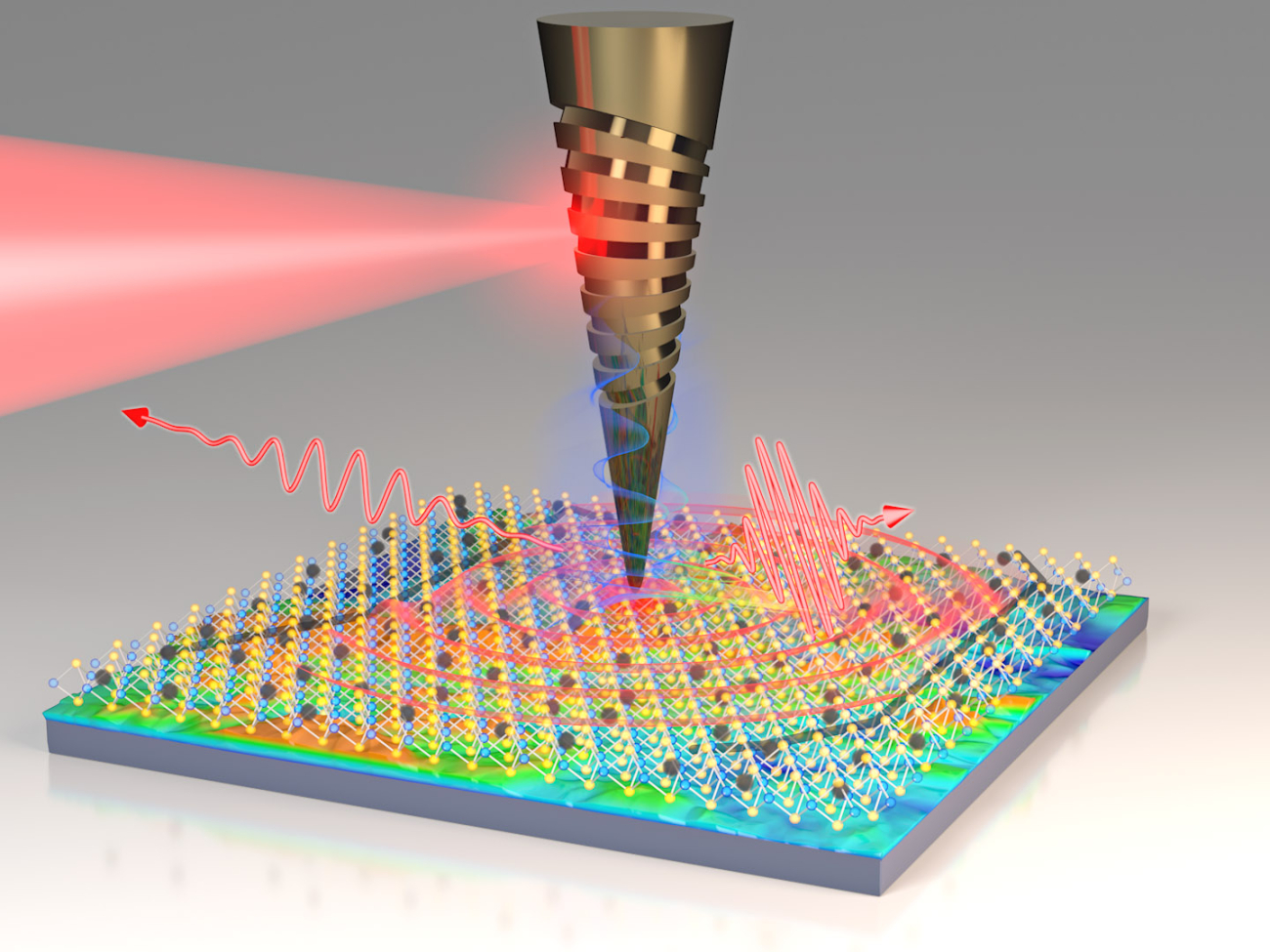
To overcome these limitations, many researchers utilize AFM (atomic force microscopy) to provide information on topography, mechanical properties, and electrical conductivity of 2D materials with nanometer-scale resolution. However, AFM by itself limits what the researcher can study, constraining how much of the quantum interactions within the materials can be observed. So Raschke and his team devised a technique to use metallic AFM tips to focus laser light down to the 10-nm scale needed to be able to image optical and dynamic properties with the same resolution with which a typical AFM can image the static mechanical properties of a material.
Exciting Excitons
The specific material Raschke and his team studied is a monolayer of tungsten diselenide (WSe2), a transition metal dichalcogenide that possesses unique electronic and photonic dynamics. “We are looking at the elementary processes of light-matter interaction in these systems,” elaborated postdoctoral researcher, and first author, Wenjin Luo. “We then use ultrafast femtosecond laser pulses that we focus to the nanoscale to locally excite excitons.” A femtosecond is 10-15, or one quadrillionths of a second, which is astonishingly fast. The researchers then observed the excitons, which are a type of elementary quantum excitation of bound electrons specific to semiconductors. One of the long-unsolved puzzles in the field of 2D semiconductors has been how these excitons react to imperfections in the semiconductor material.
To study both the dynamic behavior of these excitons and how they respond to nanoscale defects in the material, the researchers utilized a nonlinear optical process known as four-wave mixing. As Luo explained: “It is a nonlinear optical effect in which three photons of light interact with the exciton coherently and generate a fourth signal photon which we detect. This process only occurs when we use short, coherent, and intense laser pulses.” Coherence occurs when things move in sync, such as the excitons when driven by the laser field. When studying a large ensemble of excitons in conventional spectroscopy, the excitons rapidly lose their coherence due to scattering on the defects. However, “what we observe is that the coherence time of the excitons can be more than an order of magnitude longer when probing on the nanoscale,” Raschke added.
Creating an Ultrafast Image
Besides the ultrafast laser system, the key component of the imaging system was the tiny tip of the AFM which the laser had to hit. As Whetten explained: “We fabricated these optical scanning probe tips ourselves. Those are unique optical devices in their own right. The tips are first etched electrochemically from a gold wire in a multi-step process. Then we used focused ion beam milling to write a grating onto the tip shaft to couple the femtosecond pulse [to the imaging]. Only once all that's prepared can we bring in the femtosecond pulse. We then illuminate this grating on the tip shaft, and the light pulse gets focused down to the apex. The image is then created when we measure the sample point by point.”
With the point-by-point coherent imaging process, the researchers created a high-resolution image of the exciton coherence and how this coherence varies with the imperfections in the sample’s surface. This process could give other scientists the information needed to develop more efficient 2D materials. “To measure their optical properties has conventionally been limited by the diffraction limit of light capping the resolution at about 500 nanometers or so,” Whetten added. “This is insufficient to resolve [differences in the surface in] the optical properties associated with defects and grain boundaries. Our method can image with up to 100 times higher spatial resolution than was previously possible.”
This “coherent nanoscope” allowed for better spatial resolution imaging of the sample, and thanks to the ultrafast lasers, it can measure excitons at the extremely fast time scales of the elementary processes of the motion of electrons. This has significant implications for imaging samples even at room temperature, where historically experiments are carried out at low temperatures to slow the motion of excitons down. With the coherent nanoscope’s extremely high time resolution of just a few femtoseconds, Raschke, Luo, and Whetten could image the exciton dynamics even under conditions where 2D materials would typically be used in real-world applications.
Looking at Imperfections
The researchers found that the dynamics of excitons varied spatially within the material, losing the coherence fast in some areas, and with longer coherence time in others. “To get a visual picture of that, you can imagine a lawn, where the grass does not grow evenly, fast in some but slow in other areas,” Raschke explained.
Because different surfaces in a 2D material can affect its performance, visualizing where these imperfections are can help scientists develop materials with fewer heterogeneities. “This is a burgeoning field where there are all these promises of amazing technologies and new semiconductor devices, and we can look at exactly what limits we can push them to,” elaborated Whetten. “We can ask: How clean do they need to be, and what happens if they’re not perfect? How does that affect the electronic and optical behavior of a semiconductor? And imaging the exciton coherence is the most elementary process allowing us to answer these questions.”
When the team used their imaging system to study these imperfections, they discovered something surprising. “Another big takeaway was that we also saw a completely novel and nonintuitive behavior of the nonlinear optical signal itself associated with the defects,” Whetten explained. “Normally, for sample regions with long [exciton] coherence, we would have expected the strongest signal because the longer the electrons oscillate in phase, the more coherent light they would radiate. But we saw the exact opposite. With the help of our theory collaborator from Texas A&M, Alexey Belyanin, we could explain this new effect. It has to do with spatial coherence, i.e., not just how the electrons start to oscillate out of sync as time progresses, but how their spatial correlation is modified due to defects and grain boundaries.
Incorporating Belyanin’s theory, the researchers found new models to describe what affects the coherence time between excitons. “So, our work not only shows how defects limit coherence, leading to the desire to have samples with low defect densities,” added Raschke. “But it also shows that through specific defect densities, we could engineer the interplay between coherence time and signal intensity in new ways as desirable for specific nano-photonic applications.” Raschke and his team found that they could exploit the material’s imperfections to tweak the coherency times between excitons. Raschke added: “Unfortunately, we do not yet know the exact nature of the specific defects, and how different types of defect or disorder would influence the spatio-temporal coherence as it is called.” This nature is what the team will try to discover in their future work while imaging different materials, semiconductors, and quantum devices to better understand the detrimental and beneficial effects of the different defects for improved materials' function and device performance.
Written by Kenna Hughes-Castleberry, JILA Science Communicator